Fabrication of nanomaterials and metamaterials by femtosecond laser processing
Abstract
�$B!!�(BFemtosecond laser processing is topic since 1990s. Which is thought to
have following advantages;
- Thermal damage is supressed.
- Processing of wide-bandgap materials is possible.
On the other hand, "interfering femtosecond laser processing" is a topic of interest for over 10 years.
- Material surface is processed according to interference pattern.
- The period is accurate an controllable.
We started the thin film processing by interfering femtosecond laser in
early 2000s, and quite characteristic structures, such as nanobump, nanobit,
nanowaterdrop, nanowhisker, nanomesh (MHA: metal hole array) etc. in matrix,
were fabricated in a single shot, as shown in the following picture. Liquid
metal in nanosize are induced in the process, then freeze. This new technique
opens the new aspect of nanotechnology.
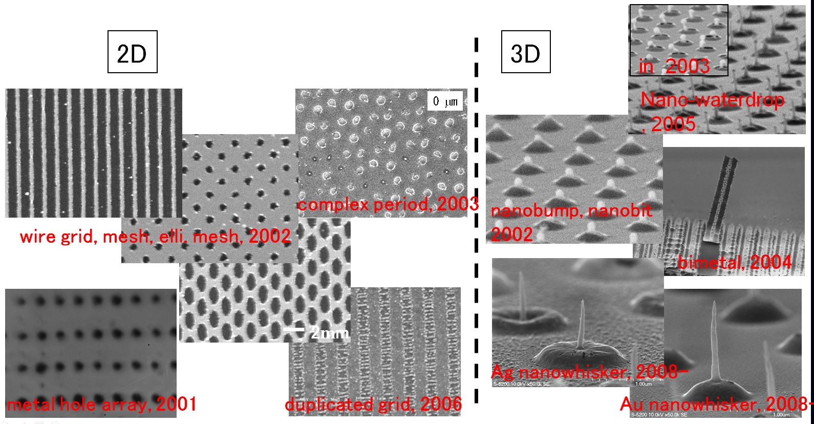
first publication of nanomesh and nanobelt etc. on: Appl. Phys. Lett. 81 (2002) 4239.
first publication of nanobump and nanowaterdrop: JP PAT submitted on 13 May, 2003, paper on JJAP submitted on 17 Sep., 2003, in Japanese in 2002.
first publication of nanowhisker: SPIE newsroom published online on 10 Jul. 2009,
-first publication of gold thin film processing and deposition by femtosecond
laser (LIFT); Kyushu Chapter of JSAP, Nov. 1997.
Outlines of research
- 1. Fabrication of new periodic nanomaterials by interfering femtosecond
laser processing
- �$B!!�(BCharacteristic nanomaterials in period can be formed via thermal process
of liquid metal. The parameters are laser and target, and various nano-structures
in matrix can be fabricated in a single shot.
- 2. Development of interfering femtosecond laser processing machine
- �$B!!�(BWe are developing a setup for interfering laser processing optimized to
ultra-short pulse laser. A laser beam is split by a DOE (Diffractive Optical
Element),and interfered on a target surface by a demagnification system
as a beam correlator. The setup is simple, and optical delay is automatically
adjusted.
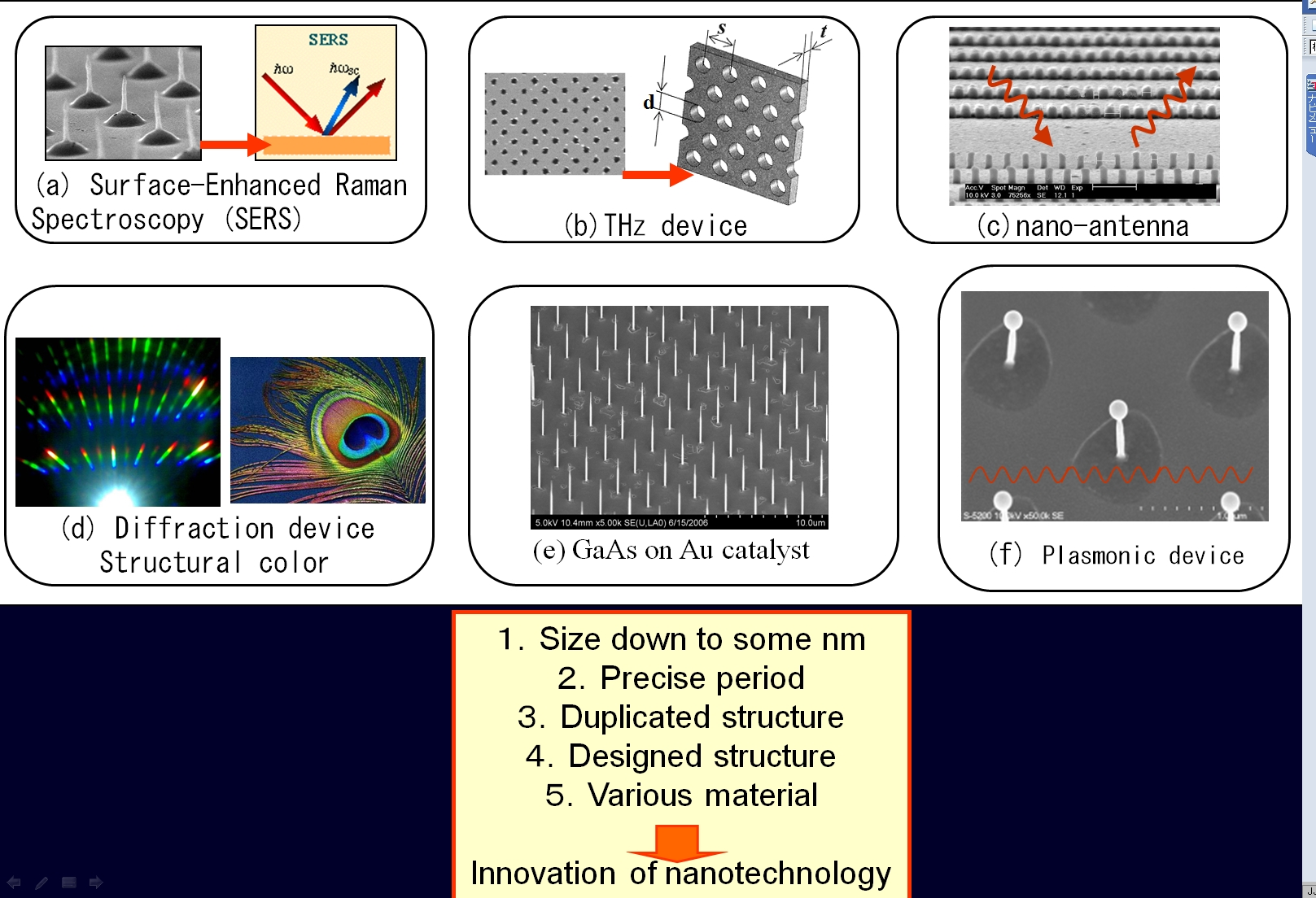
- 3. Applications
- �$B!!�(BPeriodic nanostructures have many applications as shown in the pictures
below. New nanomaterials fabricated by our technique open new aspect of
nanotechnology.
Search our papers by keywords
Please use keywords as follows (Web of Science)
Name: Nakata Y
Keywords: laser and (processing or ablation or deposition or fluorescence
or petawatt)
Affiliation: Osaka university or Kyushu university
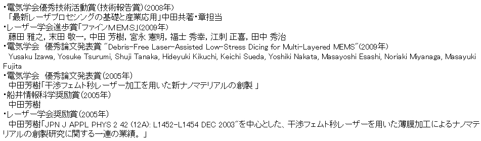
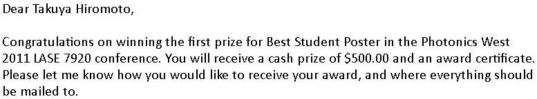
Award
2011 Photonics West Best Student Poster to Takuya Hiromoto (M2, 2011)
Awards from Japanese institutions: