
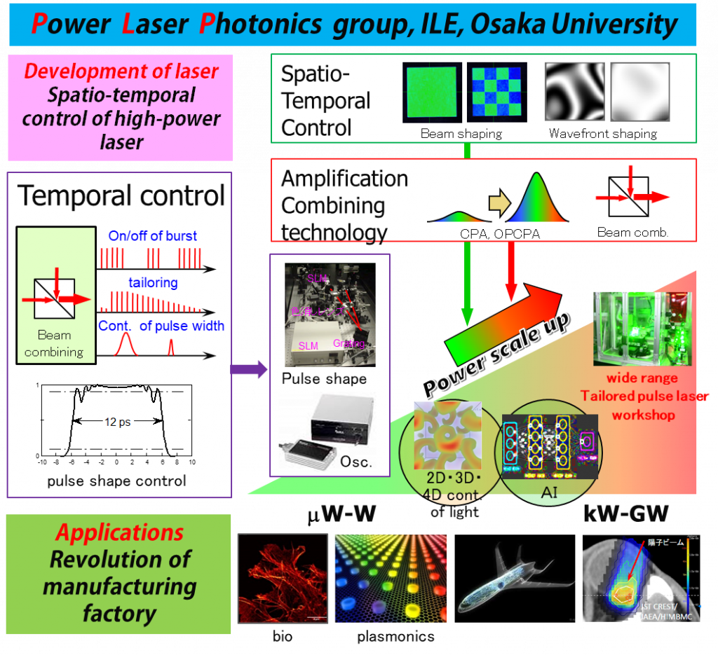
Power Laser Photonics (PLP)
Summary
We are in a cooperative group of the Electrical Engineering, Division of Electrical, Electronic and Information Engineering, Graduate School of Engineering in The University of Osaka. Our lab. is located in Institute of Laser Engineering (ILE), The University of Osaka. We investigate high-power laser and its application in cooperation with collaborative labs.
As concerning of the development of high power laser, control of spatio-temporal distribution of light-laser, high-rep. rate and high power laser have been investigated. These technologies are applied to the revolution of manufacturing industry and medical biotechnology which contribute to the foundation of the secure and safety society. The results are presented in domestic and int. conferences, published in academic journals, and used for patent acquisition. These activities contribute to our society, and develop the skills of student in doctoral courses.
Detailed information is on the website.
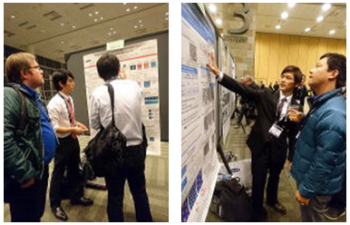
Picture 2 Poster presentation of master course students@Moscone convention center, San Francisco, USA
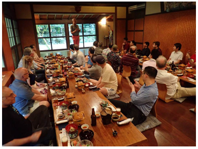
Picture 3 Banquet with international researchers@ Ishigaki island, Okinawa, Japan
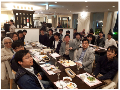
Picture 4 Welcome party. April 2018 @ Senri-Hankyu Hotel
Research topics
Laser development 1: few cycle laser with some TW peak power
Ultra-high power few cycle laser is possible to be constructed on the basis of optical-parametric chirped-pulse amplification (OPCPA) by high-repetition solid-state laser. The target spec. are (three cycle of photoelectric field oscillation), peak power30TW, rep. rate =10Hz. (1fs= 10>-15sec., 1TW = 1012 W)
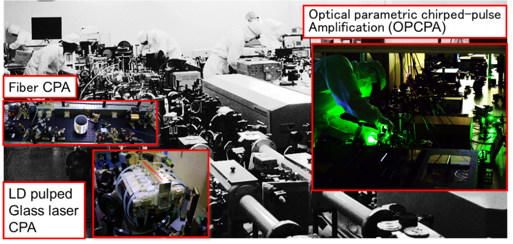
Picture 5 development of few cycle laser with some TW peak power
Laser development 2: high-power fiber laser and beam combining
Fiber laser is a very good light source for its beam quality, amplification factor and stability etc.. On the other hand, the energy is restricted due to damage threshold and disturbance by nonlinear effect such as stimulated Raman scattering and stimulated Brillouin scattering. To overcome this limitation, photonic-crystal fiber (PCF) was employed to achieve 150 W output with ps pulse width. In addition, averaged power of 1kW was achieved by coherent combining of 8 beams. Moreover, a high-power laser with controlled burst beam and free on/off control by using further beam combining is under development.
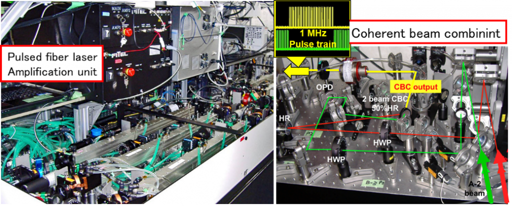
Picture 6 high-power fiber laser and coherent beam combining technology for temporally controled burst pulses.
Laser development 3: sub-ns ultraviolet high power laser
Original nonlinear crystal cooling system enabled to achieve world’s highest output of 3rd harmonic frequency conversion output. The wavelength was 347nm, pulse width was 285ps, averaged power was 300W, and the conversion efficiency was 40%.
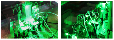
Picture 7 high-averaged power sub-ns ultraviolet pulse laser
Laser development 4: Spatial Light Modulator (SLM) and 4f system for beam shaping with ultra-high accuracy
The potential of a laser can be fully performed in fields of laser processing, bio, medical applications etc.. by beam shaping with ultra-high accuracy. In this experiment, Spatial Light Modulator: SLM and 4f system consists of two convex lenses achieved beam shaping with ultra-high accuracy, which is far beyond the ability of basic techniques such as filtering, superimposing beams etc.. In LAMOM conference 2017, master course student won a prize of poster presentation (awarded $ 500).
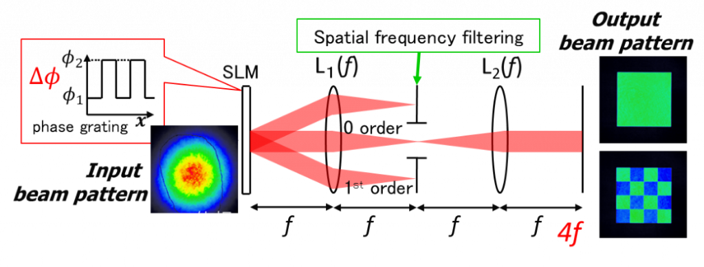
Picture 8 Spatial light modulator (SLM) and 4f system combination for beam shaping with ultra-high accuracy.
Laser application 1: laser processing contributes to the revolution of manufacturing industry
Building new sustainable society on effective use of resources and new industry, in which new materials and structures and their combinations are applied, is desired. We aim to revolutionize manufacturing industry by using super-functional and high-power laser with spatio-temporal control with high accuracy.
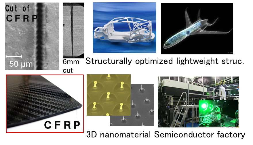
Picture 9 Revolution of manufacturing industry by spatially and temporally controlled high-functional and high power laser
Laser application 2: Creation of new nanomaterials by laser interference pattern processing
An interference pattern of laser is used in metrology and optics. In our lab., thousands to hundreds thousands nanostructures in matrix could be fabricated in milisecond timescale by liquidly behavior of metal induced by an interference pattern of high-power laser, which is called as Solid-Liquid-Solid (SLS) process. The nanomaterials are applied to plasmonic and bionic applications.
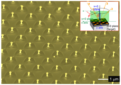
Picture 10 Creation of new nanomaterials: gold nanodrop matrix
Laser application 3: Free control of interference pattern and its application to material processing and bio applications
Control in phase and amplitude of laser is applied to the control of interference pattern, and 2D, 3D and 4D distribution of light was controlled successfully. This technique is applied to material processing, functional surface texturing and fabrication of new 3D structure etc..
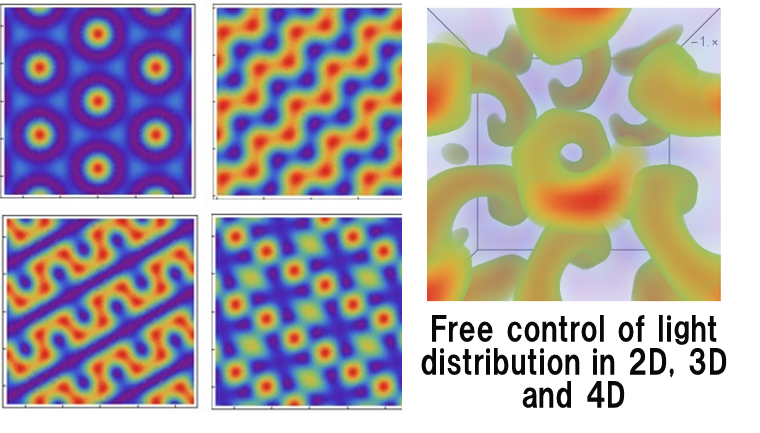
Picture 11 Control of interference pattern: distribution of light in 2D, 3D and 4D
Members
| NAKATA Yoshiki | Associate Professor |
| YOSHIDA Hidetsugu | Specially Appointed Researcher |
| KAWASAKI Tetsuji | Special case commissioned technical staff |
| SHIRAGA Hiroyuki | Guest Professor/Professor Emeritus |
| FUJITA Masayuki | Guest Professor |
| TANIGUCHI Seiji | Guest Associate Professor |